推挽缓冲电路设计(Snubber Circuits)
Push-Pull Snubber Circuit Design
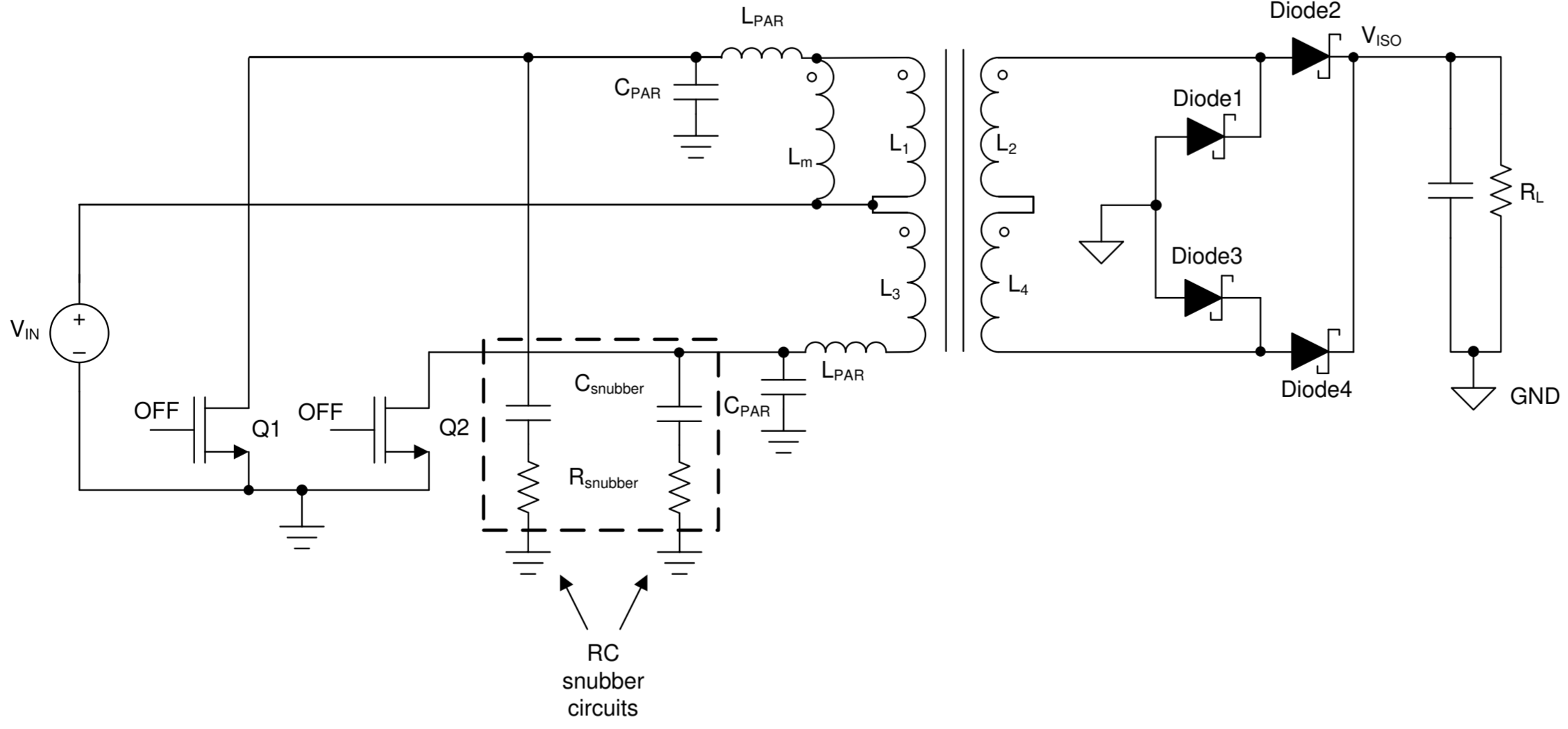
获取变压器参数和PCB参数
Obtain Transformer and PCB Parameters
测试变压器初级电感L和初级漏感Lm:次级开路,用LCR测试初级电感为L;次级短路,用LCR测试初级电感为漏感Lm。
测试变压器初级电容和次级电容:使用LCR测试初级和次级的分布电容。
去掉变压器,MOS管不上电,用LCR测试初级电感脚位的电容为PCB分布电容。
Measure the primary inductance L and primary leakage inductance Lm of the transformer: With the secondary open-circuited, measure the primary inductance using an LCR meter to obtain L; with the secondary short-circuited, measure the primary inductance using the LCR meter to get the leakage inductance Lm.
Measure the primary and secondary capacitances of the transformer: Use the LCR meter to measure the distributed capacitances of the primary and secondary windings.
Remove the transformer and do not power the MOSFET. Measure the capacitance at the primary inductance terminals using the LCR meter to obtain the PCB distributed capacitance.
计算RC——方法一
Calculating RC - Method One
测试初级(MOS的D端)的电压波形,确认脉冲振荡频率fr1。
测试未上电时,焊上变压器后,使用LCR测试初级(MOS的D端)的分布电容Cpar。
计算计生电感Lpar:$L_{par}=\frac{1}{(2\pi fr)^2C_{par}}$。
计算特征阻抗:$Z=\sqrt{\frac{L_{par}}{C_{par}}}$。
Measure the voltage waveform at the primary side (the D terminal of the MOSFET) to determine the pulse oscillation frequency fr1.
With the transformer soldered in place but not powered, use the LCR meter to measure the distributed capacitance Cpar at the primary side (the D terminal of the MOSFET).
Calculate the parasitic inductance Lpar: $L_{par}=\frac{1}{(2\pi fr)^2C_{par}}$.
Calculate the characteristic impedance: $Z=\sqrt{\frac{L_{par}}{C_{par}}}$.
根据经验,缓冲电路的R和C分别为: Based on experience, the values for R and C in the snubber circuit are as follows:
$R=Z$
$C=7 \sim 10 C_{par}$
rc时间常数为: The RC time constant is:
$\tau=RC=7ZC_{par}=7\sqrt{L_{par}C_{par}} > 2\pi\sqrt{L_{par}C_{par}}$
即比振荡频率要大,对于振荡信号来说相当于是个RC低通滤波器。 This means it is larger than the oscillation frequency. For oscillating signals, it essentially acts as an RC low-pass filter.
吸收电路需要在至少1个周期内完成放电,故时间常数也不能大于fs(开关频率)。 The snubber circuit needs to complete the discharge within at least one cycle, so the time constant must not be greater than fs (the switching frequency).
由于开关时会进行充放电,故在R上会消耗2次,功率为: Since charging and discharging occur during switching, power is dissipated twice across R, with the power being:
$P=2f_s\left(\frac{1}{2}C{V_{peak}}^2\right)=f_sC{V_{peak}}^2$
fs为开关频率,C为RC的电容,Vpeak为mos的D端振荡的峰值电压。根据这个功率估算电阻需要的封装大小。 Here, fs is the switching frequency, C is the capacitance in the RC circuit, and Vpeak is the peak voltage of the oscillation at the D terminal of the MOSFET. The required package size for the resistor can be estimated based on this power.
计算RC——方法二
Calculating RC - Method Two
不使用LCR仪器的情况下,只使用示波器可以进行近似计算。 Without using an LCR meter, approximate calculations can be made using only an oscilloscope.
测试初级(MOS的D端)的电压波形,确认脉冲振荡频率fr1:$fr_1=\frac{1}{2\pi\sqrt{L_{par}C_{par}}}$。
RC电路焊接0R+Cadd,即只焊接一个电容,比如100pF,测试脉冲振荡频率fr2:$fr_2=\frac{1}{2\pi\sqrt{L_{par}(C_{par}+C_{add})}}$。
计算特征阻抗R:$R=Z=\frac{1}{2\pi C_{add}f_{r1}}\left(\frac{f_{r1}^2}{f_{r2}^2}-1\right)$。
估算C:$C=\frac{2}{\pi f_{r1}R}$。
Measure the voltage waveform at the primary side (the D terminal of the MOSFET) to determine the pulse oscillation frequency fr1: $fr_1=\frac{1}{2\pi\sqrt{L_{par}C_{par}}}$.
Solder a capacitor, such as 100pF (Cadd), to the RC circuit without adding any resistance (0R), and measure the pulse oscillation frequency fr2: $fr_2=\frac{1}{2\pi\sqrt{L_{par}(C_{par}+C_{add})}}$.
Calculate the characteristic impedance R: $R=Z=\frac{1}{2\pi C_{add}f_{r1}}\left(\frac{f_{r1}^2}{f_{r2}^2}-1\right)$.
Estimate the capacitance C: $C=\frac{2}{\pi f_{r1}R}$.
计算可以使用在线工具 The calculations can be performed using the online tool.